Thirty years ago, CPUs and other specialized processors handled virtually all computation tasks. The graphics cards of that era helped to speed up the drawing of 2D shapes in Windows and applications, but served no other purpose.
Fast forward to today, and the GPU has become one of the most dominant chips in the industry.
But long gone are the days when the sole function for a graphics chip was, graphics – ironically – machine learning and high-performance compute heavily depend on the processing power of the humble GPU. Join us as we explore how this single chip evolved from a modest pixel pusher into a blazing powerhouse of floating-point computation.
At the beginning CPUs ruled all
Let's travel back to the late 1990s. The realm of high-performance computing, encompassing scientific endeavors with supercomputers, data processing on standard servers, and engineering and design tasks on workstations, relied entirely on two types of CPUs: 1) specialized processors designed for a singular purpose, and 2) off-the-shelf chips from AMD, IBM, or Intel.
The ASCI Red supercomputer was one of the most powerful around 1997, comprising 9,632 Intel Pentium II Overdrive CPUs (pictured below). With each unit operating at 333 MHz, the system boasted a theoretical peak compute performance of just over 3.2 TFLOPS (trillion floating point operations per second).

As we'll be referring to TFLOPS often in this article, it's worth spending a moment to explain what it signifies. In computer science, floating points, or floats for short, are data values that represent non-integer values, such as 6.2815 or 0.0044. Whole values, known as integers, are used frequently for calculations needed to control a computer and any software running on it.
Floats are crucial for situations where precision is paramount – especially anything related to science or engineering. Even a simple calculation, such as determining the circumference of a circle, involves at least one floating point value.
CPUs have had separate circuits for executing logic operations on integers and floats for many decades. In the case of the aforementioned Pentium II Overdrive, it could perform one basic float operation (multiply or add) per clock cycle. In theory, this is why ASCI Red had a peak floating point performance of 9,632 CPUs x 333 million clock cycles x 1 operation/cycle = 3,207,456 million FLOPS.
These figures are based on ideal conditions (e.g., using the simplest instructions on data that fits into the cache) and are rarely achievable in real life. However, they offer a good indication of the systems' potential power.

Other supercomputers boasted similar numbers of standard processors – Blue Pacific at Lawrence Livermore National Laboratory used 5808 IBM's PowerPC 604e chips and Los Alamos National Laboratory's Blue Mountain (above) housed 6144 MIPS Technologies R1000s.
To reach teraflop-level processing, one needed thousands of CPUs, all supported by vast amounts of RAM and hard drive storage. This was, and still is, due to the mathematical demands of the machines.
When we are first introduced to equations in physics, chemistry, and other subjects at school, everything is one-dimensional. In other words, we use a single number for distance, speed, mass, time, and so on. However, to accurately model and simulate phenomena, more dimensions are needed, and the mathematics ascends into the realm of vectors, matrices, and tensors.
These are treated as single entities in mathematics but comprise multiple values, implying that any computer working through the calculations needs to handle numerous numbers simultaneously. Given that CPUs back then could only process one or two floats per cycle, thousands of them were needed.
SIMD enters the fray: MMX, 3DNow! and SSE
In 1997, Intel updated the Pentium CPU series with a technology extension called MMX – a set of instructions that utilized eight additional registers inside the core. Each one was designed to store between one to four integer values. This system allowed the processor to execute one instruction across multiple numbers simultaneously, an approach better known as SIMD (Single Instruction, Multiple Data).
A year later, AMD introduced its own version called 3DNow!. It was notably superior, as the registers could store floating point values. It took another year before Intel addressed this issue in MMX, with the introduction of SSE (Streaming SIMD Extensions) in the Pentium III.

As the calendar rolled into a new millennium, designers of high-performance computers had access to standard processors that could efficiently handle vector mathematics.
Once scaled into the thousands, these processors could manage matrices and tensors equally well. Despite this advancement, the world of supercomputers still favored older or specialized chips, as these new extensions weren't precisely designed for such tasks. This was also true for another rapidly popularizing processor better at SIMD work than any CPU from AMD or Intel: the GPU.
This was also true for another rapidly popularizing processor better at SIMD work than any CPU from AMD or Intel: the GPU.
In the early years of graphics processors, the CPU processed the calculations for the triangles composing a scene (hence the 3DNow! name that AMD used for its implementation of SIMD). However, the coloring and texturing of pixels were exclusively handled by the GPU, and many aspects of this work involved vector mathematics.
The best consumer-grade graphics cards from 20+ years ago, such as the 3dfx Voodoo5 5500 and the Nvidia GeForce 2 Ultra, were outstanding SIMD devices. However, they were created to produce 3D graphics for games and nothing else. Even cards in the professional market were solely focused on rendering.

ATI's $2,000 ATI FireGL 3 sported two IBM chips (a GT1000 geometry engine and an RC1000 rasterizer), an enormous 128 MB of DDR-SDRAM, and a claimed 30 GFLOPS of processing power. But all that was for accelerating graphics in programs like 3D Studio Max and AutoCAD, using the OpenGL rendering API.
GPUs of that era weren't equipped for other uses, as the processes behind transforming 3D objects and converting them into monitor images didn't involve a substantial amount of floating point math. In fact, a significant part of it was at the integer level, and it would take several years before graphics cards started heavily operating with floating point values throughout their pipelines.
One of the first was ATI's R300 processor, which had 8 separate pixel pipelines, handling all of the math at 24-bit floating point precision. Unfortunately, there was no way of harnessing that power for anything other than graphics – the hardware and associated software were entirely image-centric.
Computer engineers weren't oblivious to the fact that GPUs had vast amounts of SIMD power but lacked a way to apply it in other fields. Surprisingly, it was a gaming console that showed how to solve this thorny problem.
A new era of unification
Microsoft's Xbox 360 hit the shelves in November 2005, featuring a CPU designed and manufactured by IBM based on the PowerPC architecture, and a GPU designed by ATI and fabricated by TSMC.
This graphics chip, codenamed Xenos, was special because its layout completely eschewed the classic approach of separate vertex and pixel pipelines.
Xenos sparked a design paradigm that remains in use today.

In their place was a three-way cluster of SIMD arrays. Specifically, each cluster consisted of 16 vector processors, with each containing five math units. This layout enabled each array to execute two sequential instructions from a thread, per cycle, on 80 floating point data values simultaneously.
Known as a unified shader architecture, each array could process any type of shader. Despite making other aspects of the chip more complicated, Xenos sparked a design paradigm that remains in use today. With a clock speed of 500 MHz, the entire cluster could theoretically achieve a processing rate of 240 GFLOPS (500 x 16 x 80 x 2) for three threads of a multiply-then-add command.
To give this figure some sense of scale, some of the world's top supercomputers a decade earlier couldn't match this speed. For instance, the aragon XP/S140 at Sandia National Laboratories, which topped the world's supercomputer list in 1994 with its 3,680 Intel i860 CPUs, had a peak of 184 GFLOPS. The pace of chip development quickly outpaced this machine, but the same would be true of the GPU.
CPUs had been incorporating their own SIMD arrays for several years – for example, Intel's original Pentium MMX had a dedicated unit for executing instructions on a vector, encompassing up to eight 8-bit integers. By the time Xbox's Xenos was being utilized in homes worldwide, such units had at least doubled in size, but they were still minuscule compared to those in Xenos.

When consumer-grade graphics cards began to feature GPUs with a unified shader architecture, they already boasted a noticeably higher processing rate than the Xbox 360's graphics chip.
Nvidia's G80 (above), as used in the GeForce 8800 GTX (2006), had a theoretical peak of 346 GLFOPS, and ATI's R600 in the Radeon HD 2900 XT (2007) boasted 476 GLFOPS.
Both graphics chip makers quickly capitalized on this computing power in their professional models. While exorbitantly priced, the ATI FireGL V8650 and Nvidia Tesla C870 were well-suited for high-end scientific computers. However, at the highest level, supercomputers worldwide continued to rely on standard CPUs. In fact, several years would pass before GPUs started appearing in the most powerful systems.
But why were GPUs weren't used straight away, when they clearly offered an enormous amount of processing speed?
Supercomputers and similar systems are extremely expensive to design, construct, and operate. For years, they had been built around massive arrays of CPUs, so integrating another processor wasn't an overnight endeavor. Such systems required thorough planning and initial small-scale testing before increasing the chip count.
Secondly, getting all these components to function harmoniously, especially regarding software, is no small feat, which was a significant weakness for GPUs at that time. While they had become highly programmable, the software previously available for them was rather limited.
Microsoft's HLSL (Higher Level Shader Language), Nvidia's Cg library, and OpenGL's GLSL made it simple to access the processing capability of a graphics chip, though purely for rendering.
That all changed with unified shader architecture GPUs.

In 2006, ATI, which by then had become a subsidiary of AMD, and Nvidia released software toolkits aimed at exposing this power for more than just graphics, with their APIs called CTM (Close To Metal) and CUDA (Compute Unified Device Architecture), respectively.
What the scientific and data processing community truly needed, however, was a comprehensive package – one that would treat enormous arrays of CPUs and GPUs (often referred to as a heterogeneous platform) as a single entity comprised of numerous compute devices.
Their need was met in 2009. Originally developed by Apple, OpenCL was released by the Khronos Group, who had absorbed OpenGL a few years earlier, to become the de facto software platform for using GPUs outside of everyday graphics or as the field was then known by, the GPGPU which referred to general-purpose computing on GPUs, a term coined by Mark Harris.
The GPU enters the compute race
Unlike the expansive world of tech reviews, there aren't hundreds of reviewers globally testing supercomputers for their supposed performance claims. However, an ongoing project that started in the early 1990s by the University of Mannheim in Germany seeks to do just that.
Known as the TOP500, the group releases a ranked list of the 10 most powerful supercomputers in the world twice a year.
The first entries boasting GPUs appeared in 2010, with two systems in China – Nebulae and Tianhe-1. These relied on Nvidia's Tesla C2050 (essentially a GeForce GTX 470, as shown in the picture below) and AMD's Radeon HD 4870 chips, respectively, with the former boasting a theoretical peak of 2,984 TFLOPS.

During these early days of high-end GPGPU, Nvidia was the preferred vendor for outfitting a computing behemoth, not because of performance – as AMD's Radeon cards usually offered a higher degree of processing performance – but due to software support. CUDA underwent rapid development, and it would be a few years before AMD had a suitable alternative, encouraging users to go with OpenCL instead.
However, Nvidia didn't entirely dominate the market, as Intel's Xeon Phi processor tried to carve out a place. Emerging from an aborted GPU project named Larrabee, these massive chips were a peculiar CPU-GPU hybrid, composed of multiple Pentium-like cores (the CPU part) paired with large floating-point units (the GPU part).
An examination of Nvidia Tesla C2050's internals reveals 14 blocks called Streaming Multiprocessors (SMs), divided by cache and a central controller. Each one includes 32 sets of two logic circuits (which Nvidia calls CUDA cores) that execute all the mathematical operations – one for integer values, and the other for floats. In the latter's case, the cores can manage one FMA (Fused Multiply-Add) operation per clock cycle at single (32-bit) precision; double precision (64-bit) operations require at least two clock cycles.
The floating-point units in the Xeon Phi chip (shown below) appear somewhat similar, except each core processes half as many data values as the SMs in the C2050. Nevertheless, as there are 32 repeated cores compared to the Tesla's 14, a single Xeon Phi processor can handle more values per clock cycle overall. However, Intel's first release of the chip was more of a prototype and couldn't fully realize its potential – Nvidia's product ran faster, consumed less power, and proved to be ultimately superior.

This would become a recurring theme in the three-way GPGPU battle among AMD, Intel, and Nvidia. One model might possess a superior number of processing cores, while another might have a faster clock speed, or a more robust cache system.
While a single CPU couldn't compete with the SIMD performance of an average GPU, when connected together in the thousands, they proved adequate. However, such systems lacked power efficiency.
CPUs remained essential for all types of computing, and many supercomputers and high-end computing systems still consisted of AMD or Intel processors. While a single CPU couldn't compete with the SIMD performance of an average GPU, when connected together in the thousands, they proved adequate. However, such systems lacked power efficiency.
For example, at the same time that the Radeon HD 4870 GPU was being used in the Tianhe-1 supercomputer, AMD's biggest server CPU (the 12-core Opteron 6176 SE) was going the rounds. For a power consumption of around 140 W, the CPU could theoretically hit 220 GFLOPS, whereas the GPU offered a peak of 1,200 GFLOPS for just an extra 10 W, and at a fraction of the cost.
A little graphics card that could (do more)
A few years later and it wasn't only the world's supercomputers that were leveraging GPUs to conduct parallel calculations en masse. Nvidia was actively promoting its GRID platform, a GPU virtualization service, for scientific and other applications. Originally launched as a system to host cloud-based gaming, the rising demand for large-scale, affordable GPGPU made this transition inevitable. At its annual technology conference, GRID was presented as a significant tool for engineers across various sectors.
In the same event, the GPU maker provided a glimpse into a future architecture, codenamed Volta. Few details were released, and the general assumption was that this would be another chip serving across all of Nvidia's markets.

Meanwhile, AMD was doing something similar, utilizing its regularly updated Graphics Core Next (GCN) design in its gaming-focused Radeon lineup, as well as its FirePro and Radeon Sky server-based cards. By then, the performance figures were astonishing – the FirePro W9100 had a peak FP32 throughput of 5.2 TFLOPS (32-bit floating point), a figure that would have been unthinkable for a supercomputer less than two decades earlier.
GPUs were still primarily designed for 3D graphics, but advancements in rendering technologies meant that these chips had to become increasingly proficient at handling general compute workloads. The only issue was their limited capability for high-precision floating-point math, i.e., FP64 or greater.
Looking at the top supercomputers of 2015 shows a relatively small number using GPUs, either Intel's Xeon Phi or Nvidia's Tesla, compared to those that were entirely CPU-based.
That all changed when Nvidia launched the Pascal architecture in 2016. This was the company's first foray into designing a GPU exclusively for the high-performance computing market, with others being used across multiple sectors. Only one of the former was ever made (the GP100) and it spawned only 5 products, but where all previous architectures only sported a handful of FP64 cores, this chip housed nearly 2,000 of them.
With the Tesla P100 offering over 9 TFLOPS of FP32 processing and half that figure for FP64, it was seriously powerful. AMD's Radeon Pro W9100, using the Vega 10 chip, was 30% faster in FP32 but 800% slower in FP64. By this point, Intel was on the brink of discontinuing Xeon Phi due to poor sales.
A year later, Nvidia finally released Volta, making it immediately apparent that the company wasn't solely interested in introducing its GPUs to the HPC and data processing markets – it was targeting another one as well.
Neurons, networks, oh my!
Deep Learning is a field within the broader set of disciplines known as Machine Learning, which in turn is a subset of Artificial Intelligence. It involves the use of complex mathematical models, known as neural networks, that extract information from given data.
An example of this is determining the probability that a presented image depicts a specific animal. To do this, the model needs to be 'trained' – in this example, shown millions of images of that animal, along with millions more that do not show the animal. The mathematics involved is rooted in matrix and tensor computations.
For decades, such workloads were only suitable for massive CPU-based supercomputers. However, as early as the 2000s, it was apparent that GPUs were ideally suited for such tasks.
Nevertheless, Nvidia gambled on a significant expansion of the deep learning market and added an extra feature to its Volta architecture to make it stand out in this field. Marketed as tensor cores, these were banks of FP16 logic units, operating together as a large array, but with very limited capabilities.

In fact, they were so limited that they performed just one function: multiplying two FP16 4x4 matrices together and then adding another FP16 or FP32 4x4 matrix to the result (a process known as a GEMM operation). Nvidia's previous GPUs, as well as those from competitors, were also capable of performing such calculations but nowhere near as quickly as Volta. The sole GPU made using this architecture, the GV100, housed a total of 512 tensor cores, each capable of executing 64 GEMMs per clock cycle.
Depending on the size of the matrices in the dataset, and the floating point size used, the Tesla V100 card could theoretically reach 125 TFLOPS in these tensor calculations. Volta was clearly designed for a niche market, but where the GP100 made limited inroads into the supercomputer field, the new Tesla models were rapidly adopted.
PC enthusiasts will be aware that Nvidia subsequently added tensor cores to its general consumer products in the ensuing Turing architecture, and developed an upscaling technology called DLSS (Deep Learning Super Sampling), which uses the cores in the GPU to run a neural network on an upscaling image, correcting any artifacts in the frame.
For a brief period, Nvidia had the GPU-accelerated deep learning market to itself, and its data center division saw revenues surge – with growth rates of 145% in FY17, 133% in FY18, and 52% in FY19. By the end of FY19, sales for HPC, deep learning, and others totaled $2.9 billion, which was a very positive result.
But then, the market really exploded. The company's total earnings for the final quarter of 2023 came in at $22.1 billion, a staggering 265% rise year-over-year. The majority of that growth came from the company's AI initiatives, which generated $18.4 billion in revenues.

However, where there's money, competition is inevitable and even though Nvidia remains by far the top GPU provider, other big tech companies are not sitting still.
In 2018, Google began offering access to its own tensor processing chips, which it had developed in-house, via a cloud service. Amazon soon followed suit with its specialized CPU, the AWS Graviton. Meanwhile, AMD was restructuring its GPU division, forming two distinct product lines: one predominantly for gaming (RDNA) and the other exclusively for computing (CDNA).
While RDNA was notably different from its predecessor, CDNA was very much a natural evolution of GCN, albeit one scaled to an enormous level. Looking at today's GPUs for supercomputers, data servers, and AI machines, everything is enormous.
AMD's CDNA 2-powered MI250X sports 220 Compute Units, providing just under 48 TFLOPS of double-precision FP64 throughput and 128 GB of High Bandwidth Memory (HBM2e), with both aspects being much sought after in HPC applications. Nvidia's GH100 chip, using its Hopper architecture and 576 Tensor Cores, can potentially hit 4000 TOPS, with the low-precision INT8 number format in AI matrix calculations.
However, one thing they all share is what they are decidedly not – they are not GPUs.
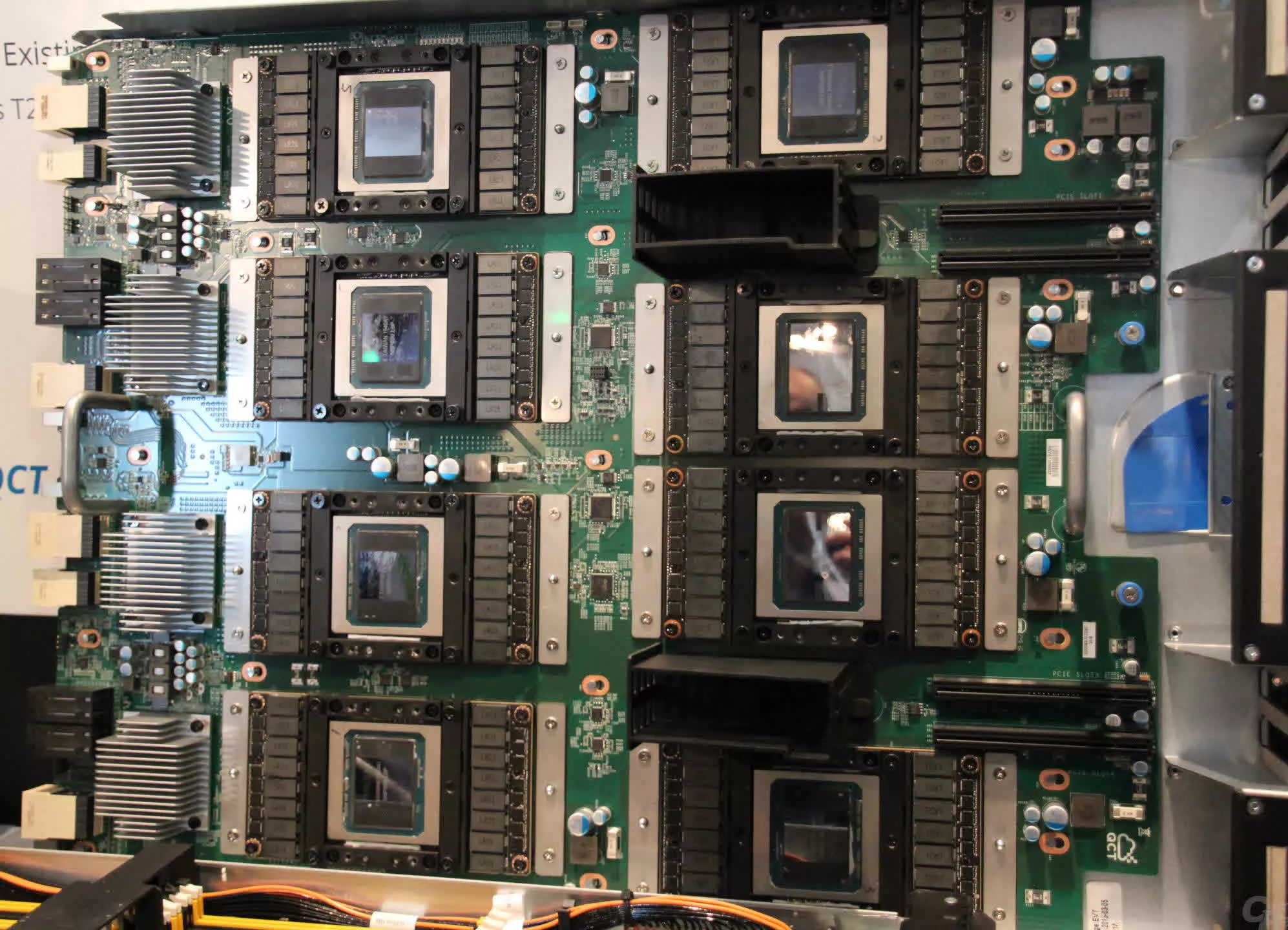
Intel's Ponte Vecchio GPU is equally gargantuan, with 100 billion transistors, and AMD's MI300 has 46 billion more, comprising multiple CPU, graphics, and memory chiplets.

However, one thing they all share is what they are decidedly not – they are not GPUs. Long before Nvidia appropriated the term as a marketing tool, the acronym stood for Graphics Processing Unit. AMD's MI250X has no render output units (ROPs) whatsoever, and even the GH100 only possesses the Direct3D performance of something akin to a GeForce GTX 1050, rendering the 'G' in GPU irrelevant.
So, what could we call them instead?
"GPGPU" isn't ideal, as it is a clumsy phrase referring to using a GPU in generalized computing, not the device itself. "HPCU" (High Performance Computing Unit) isn't much better. But perhaps it doesn't really matter.
After all, the term "CPU" is incredibly broad and encompasses a wide array of different processors and uses.
What's next for the GPU to conquer?
With billions of dollars invested in GPU research and development by Nvidia, AMD, Apple, Intel, and dozens of other companies, the graphics processor of today isn't going to be replaced by anything drastically different anytime soon.
For rendering, the latest APIs and software packages that use them (such as game engines and CAD applications) are generally agnostic toward the hardware that runs the code, so in theory, they could be adapted to something entirely new.
There are relatively few components within a GPU dedicated solely to graphics... the rest is essentially a massively parallel SIMD chip, supported by a robust and intricate memory system.
However, there are relatively few components within a GPU dedicated solely to graphics – the triangle setup engine and ROPs are the most obvious ones, and ray tracing units in more recent releases are highly specialized, too. The rest, however, is essentially a massively parallel SIMD chip, supported by a robust and intricate memory/cache system.

The fundamental designs are about as good as they're ever going to get and any future improvements are simply tied to on advances in semiconductor fabrication techniques. In other words, they can only improve by housing more logic units, running at a higher clock speed, or a combination of both.
Of course, they can have new features incorporated to allow them to function in a broader range of scenarios. This has happened several times throughout the GPU's history, though the transition to a unified shader architecture was particularly significant. While it's preferable to have dedicated hardware for handling tensors or ray tracing calculations, the core of a modern GPU is capable of managing it all, albeit at a slower pace.
This is why the likes of the AMD MI250 and Nvidia GH100 bear a strong resemblance to their desktop PC counterparts, and future designs intended for use in HPC and AI are likely to follow this trend. So if the chips themselves aren't going to change significantly, what about their application?

Given that anything related to AI is essentially a branch of computation, a GPU is likely to be used whenever there's a need to perform a multitude of SIMD calculations. While there aren't many sectors in science and engineering where such processors aren't already being utilized, what we're likely to see is a surge in the use of GPU-derivatives.
One can currently purchase phones equipped with miniature chips whose sole function is to accelerate tensor calculations. As tools like ChatGPT continue to grow in power and popularity, we'll see more devices featuring such hardware.
The humble GPU has evolved from a device merely intended to run games faster than a CPU alone could, to a universal accelerator, powering workstations, servers, and supercomputers around the globe.
The humble GPU has evolved from a device merely intended to run games faster than a CPU alone could, to a universal accelerator, powering workstations, servers, and supercomputers around the globe.
Millions of people worldwide use one every day – not just in our computers, phones, televisions, and streaming devices, but also when we utilize services that incorporate voice and image recognition, or provide music and video recommendations.
What's truly next for the GPU may be uncharted territory, but one thing is certain, the graphics processing unit will continue to be the dominant tool for computation and AI for many decades to come.